What is HBM memory, and why does AI need so much of it?
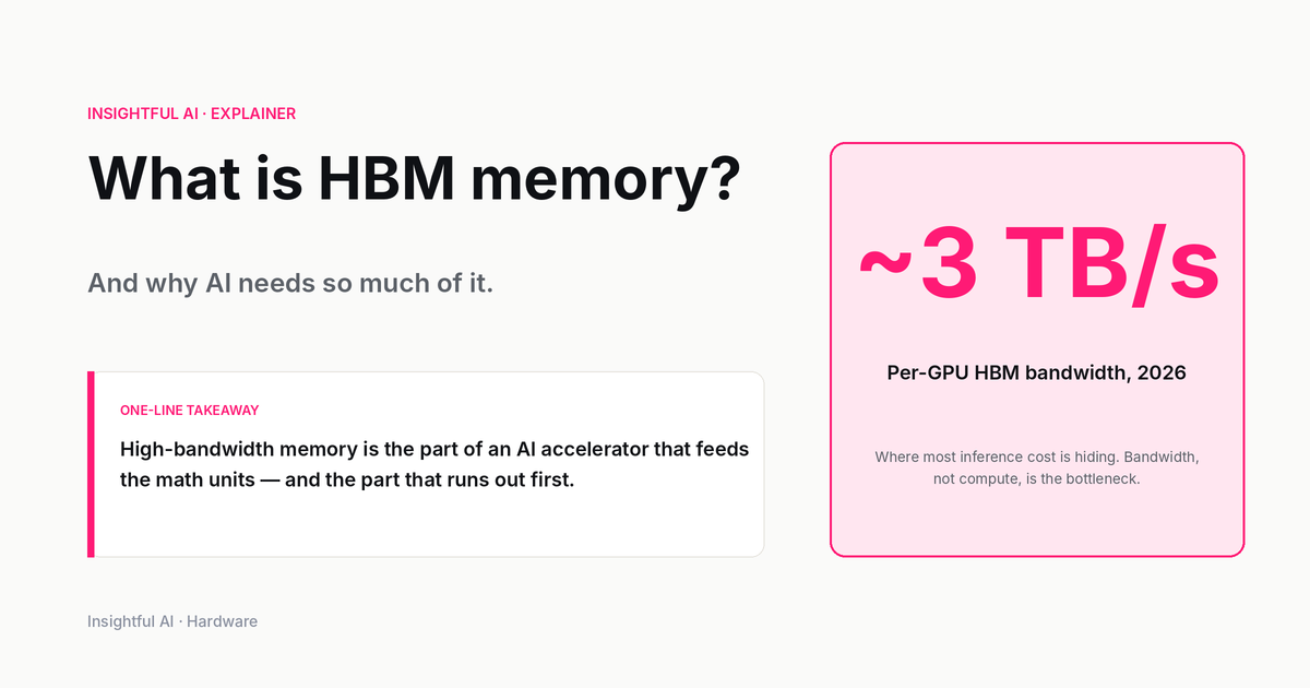
HBM is the high-bandwidth memory glued to every modern AI accelerator — and the single component most likely to be the bottleneck the next time someone says 'we need more GPUs.'
By Alex Chen, Insightful AI Desk
Every modern AI accelerator ships with a pile of memory bonded to the same silicon package as the compute die. Tens of gigabytes per stack, several stacks per package, hundreds of gigabytes per server, petabytes across a training cluster. None of this is DRAM in the conventional sense, and none of it sits on a separate board the way your laptop’s RAM does. It is HBM, or high-bandwidth memory, and it is the component most likely to be the bottleneck the next time someone in the room says “we need more GPUs.”
HBM is also the part of the AI stack that least resembles its press releases. Vendor announcements quote eye-watering bandwidth numbers but rarely mention that only three companies in the world produce HBM at volume, that allocations are signed years in advance, or that the chip you actually receive depends on a packaging process whose yield is a closely held secret. If you are trying to read the AI supply chain, or just understand why a GPU costs what it costs, HBM is the line item to study.
What HBM actually is

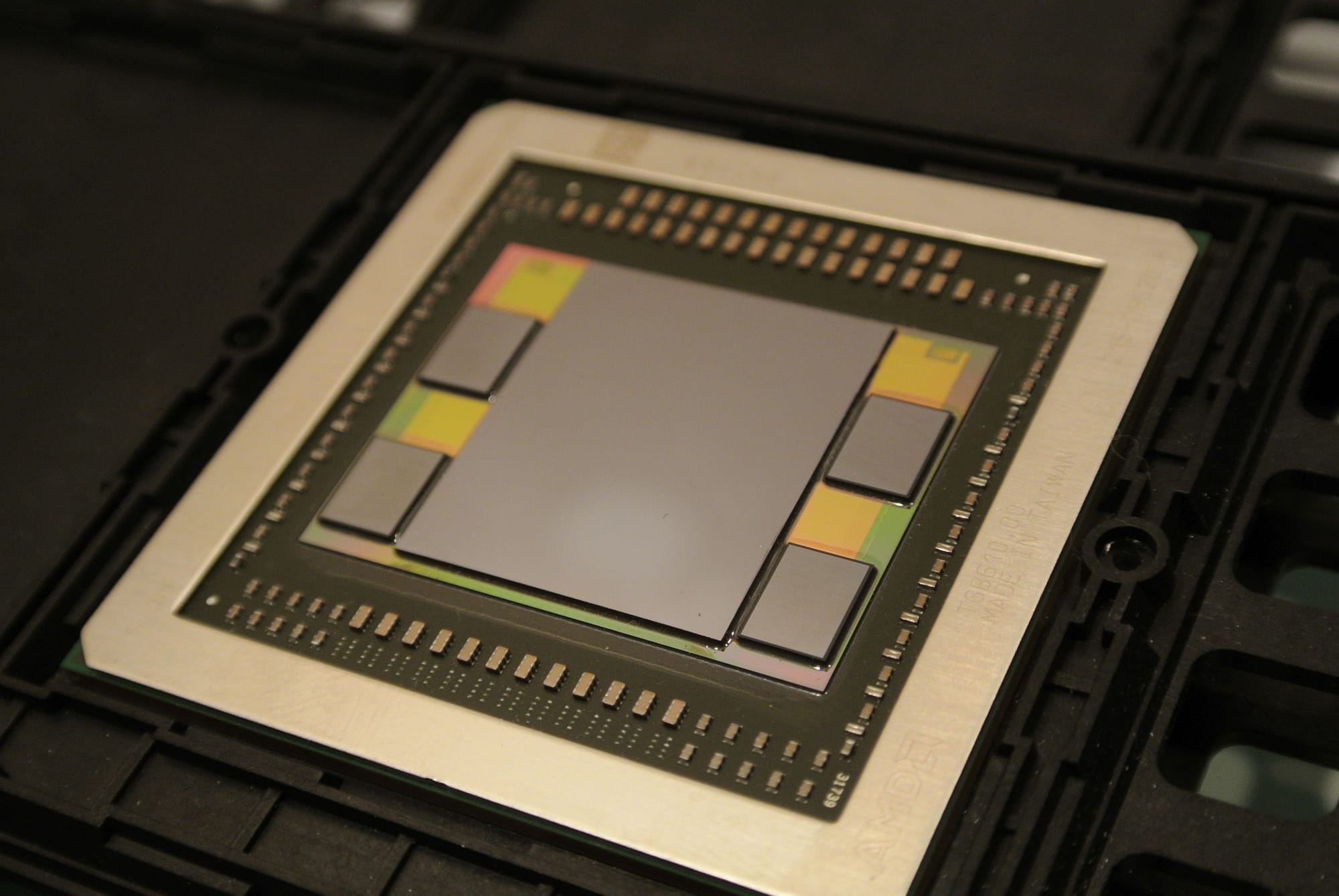
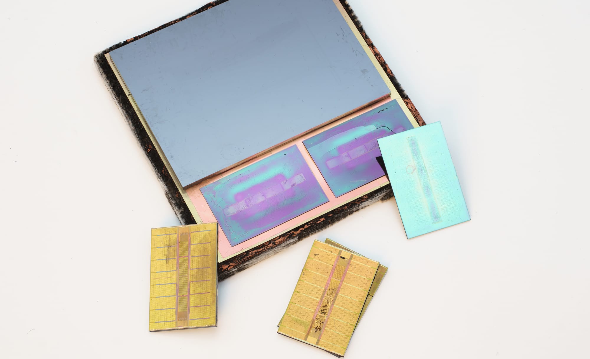
HBM is DRAM, the same basic memory technology that has been in computers for decades, rearranged into a vertical stack and placed millimetres away from a GPU die instead of on a separate motherboard component. A single HBM “cube” (the industry term for one stack) contains several individual DRAM dice piled on top of each other, connected by tiny vertical wires called through-silicon vias, or TSVs. The whole stack sits on a base logic die that handles the interface to the GPU.
Those stacks do not connect to the GPU through the kind of trace you would find on a normal printed circuit board. Instead, they share a passive piece of silicon called an interposer, which acts as an extremely dense wiring substrate. A modern GPU package (the actual rectangle you would hold in your hand) contains the compute die, four to eight HBM stacks, and the interposer that wires them together, all behind a single heat spreader. From the outside it looks like one chip. Inside, it is a small city.
The geometry matters because it explains the bandwidth. A normal DDR memory bus has, say, 64 to 128 wires running between the CPU and the memory module. An HBM stack uses a 1,024-bit interface, eight to sixteen times wider, and runs that interface at multi-gigabit-per-second speeds. Wider plus faster equals an order-of-magnitude more bytes per second flowing between memory and compute, which is exactly what large language models need.
Why GPUs need it
Training and serving a modern AI model is, at the level of cycles and bytes, mostly a memory-bandwidth problem dressed up as a compute problem.
A transformer model with tens of billions of parameters does not fit inside the GPU’s on-die cache. The weights have to be loaded from somewhere, used in a matrix multiply, and then often loaded again for the next layer. The compute units, the parts vendors put on slides, can do trillions of operations per second, but only if data arrives fast enough to keep them busy. If the memory bus is too narrow or too slow, the compute units stall and you have paid for silicon that is idle.
Conventional DDR memory cannot keep up. Even the latest DDR5 generation delivers tens of gigabytes per second per channel; an AI workload needs an order of magnitude more, sustained, with low enough latency that pipeline bubbles do not accumulate. HBM is the answer the industry settled on. By putting wide, fast memory physically adjacent to the compute, the bandwidth wall moves out far enough that the compute units actually have a chance to stay fed.
This is why “memory bandwidth” has become a headline spec on every AI accelerator launch. Not because it is new, but because it is the constraint that everything else gets engineered against.
The generations: what the numbers mean
HBM is standardised by JEDEC, the industry body that maintains memory specifications. Each generation has a formal document number and a public release date. Below are the figures cited in the JEDEC standards as summarised on Wikipedia’s HBM page, which compiles the per-stack bandwidth, per-pin transfer rate, and approximate release dates from primary documentation.
| Generation | JEDEC doc | Released | Per-pin rate | Bandwidth per stack |
|---|---|---|---|---|
| HBM | JESD235 | October 2013 | 1.0 Gb/s | 128 GB/s |
| HBM2 | JESD235A | January 2016 | 2.4 Gb/s | 256 GB/s |
| HBM2E | — | 2018–2020 | 3.6 Gb/s | 307–461 GB/s |
| HBM3 | JESD238 | January 2022 | 6.4 Gb/s | 819 GB/s |
| HBM3E | — | 2024 (production) | 9.8 Gb/s | ~1.23 TB/s |
Three things are worth noticing in that table.
First, the per-pin transfer rate roughly doubled at every generation. That is normal in semiconductors and is the same kind of curve you see in PCIe or USB. What is unusual is that the interface width (1,024 bits) stayed constant. The bandwidth gains came from running the existing wires faster, which is engineering-wise much harder than adding more wires, because faster signalling on closely packed traces creates noise and heat problems that the interposer has to absorb.
Second, the bandwidth-per-stack figure is per stack. A single accelerator package usually carries four to six stacks. The aggregate memory bandwidth on a modern AI accelerator therefore runs into the several-terabytes-per-second range, roughly an order of magnitude above the fastest CPU systems on the market.
Third, “HBM3E” is not a separate JEDEC generation. It is a pin-compatible extension of HBM3 that pushes the per-pin rate higher while keeping the rest of the protocol unchanged. The “E” is the kind of incremental upgrade that lets accelerator vendors drop in faster memory without redesigning the controller. It is also the version currently shipping in the high-volume AI parts.
Who actually makes it
HBM was co-developed at AMD beginning in 2008, with SK Hynix joining as the manufacturing partner. SK Hynix produced the first commercial HBM chip in 2013, around the time the JEDEC standard was published. The first GPU to ship with HBM was AMD’s Fiji, the silicon behind the Radeon R9 Nano.
Today, the worldwide HBM supply comes from three manufacturers: SK Hynix, Samsung, and Micron. That is the entire list. The technology is not patent-walled in the obvious sense (the JEDEC standard is public) but the manufacturing process is. Producing high-yield 3D DRAM stacks requires hundreds of millions of dollars of fab equipment, mature TSV processes, and packaging capacity that is closely tied to the same advanced fabs that produce the GPU dice they will sit next to.
For a buyer of AI infrastructure, this concentration is the supply story. When a single accelerator generation requires more HBM than the world’s combined supply can produce, the bottleneck is not the GPU vendor. It is the HBM allocation contract signed eighteen months earlier. This is why “HBM allocation” shows up as a quoted constraint in earnings calls and in news coverage of AI capacity, and why a hyperscaler’s ability to actually deploy ordered accelerators often depends on a supply chain two layers below the GPU brand on the bill of materials.
Why it matters for AI
Three concrete implications follow from the geometry above, each paired with a caveat.
HBM capacity caps the size of the model you can serve on a single GPU. An 80 GB HBM3 budget can hold roughly 40 billion parameters in 16-bit precision before any activations, optimiser states, or KV cache. Larger models have to be sharded across multiple GPUs, with the inter-GPU interconnect (NVLink, InfiniBand) handling the spillover. The caveat: quantisation and sparsity techniques materially change this math; an 8-bit or 4-bit model fits more parameters per GB. The headline 80 GB number is a constraint, not a death sentence.
HBM bandwidth caps how fast a model can serve a token. The token-generation step in inference is dominated by reading the model weights out of memory for each new token. Back-of-envelope, dividing a few TB/s of bandwidth by tens of GB of weights suggests a ceiling on the order of tens of tokens per second per sequence on a single GPU, before any batching or optimisation. Real systems batch many requests together to amortise this, which is why throughput numbers on cloud APIs tend to look better than the per-sequence math would suggest. The caveat: the actual achievable bandwidth is always lower than the spec, and batching mathematics is a discipline of its own.
HBM is the part of the supply chain that decides when AI hardware ships. If you read carefully, almost every “capacity-constrained” statement from an AI cloud provider eventually points to HBM, not to GPU dice. The caveat: packaging capacity (the step that bonds HBM stacks to the GPU die on an interposer) is often the actual binding constraint, and is distinct from raw HBM production capacity. The bottleneck moves around within the back-end of the supply chain.
What to watch next
HBM4 is the publicly announced next generation under JEDEC, expected to introduce a wider interface and higher per-pin rates than HBM3E. Specific spec figures and finalisation dates should be checked against JEDEC’s own press releases before relying on them; reporting from secondary outlets has varied. Production volumes follow JEDEC standards by roughly twelve to twenty-four months, so the parts shipping in the next generation of AI accelerators are the ones to watch.
For the non-builder, the practical signals to track are these: which fab and packaging capacity each of the three HBM suppliers is committing to for the next year; how that capacity is allocated across the major accelerator vendors; and which generation of HBM is bound to which generation of accelerator. Those three together largely determine which AI products can be deployed at what scale and when.
How to read an HBM-related announcement
If a chip vendor announces an accelerator with a quoted memory bandwidth number, three questions surface what they are really claiming.
Which HBM generation, and how many stacks? The headline number is the product of per-stack bandwidth and stack count. Knowing both tells you whether the gain came from a new generation or from packing in more stacks.
What is the total capacity in gigabytes? Bandwidth is one axis; total capacity is the other. A high-bandwidth, low-capacity part suits inference-heavy workloads. A high-capacity part suits very large models.
Who is the HBM supplier, and what is the allocation? If a vendor will not say, the answer is often “all three, in whatever ratio we can secure.” That tells you the part is supply-limited.
Most of what is interesting about an AI accelerator launch hides in the answers to those three questions, not in the slide that says “X petaflops.”
Further reading: Wikipedia’s High Bandwidth Memory article compiles the JEDEC release dates and bandwidth figures with citations to the primary standards. JEDEC’s own press releases for JESD235, JESD238, and successors are the authoritative source for any specific spec question.
How we use AI and review our work: About Insightful AI Desk.

